
The new products include the Kronos 1190 wafer-level packaging inspection system, the ICOS F160XP die sorting and inspection system and the next-generation ICOS T3/T7 Series of packaged IC component inspection and metrology systems
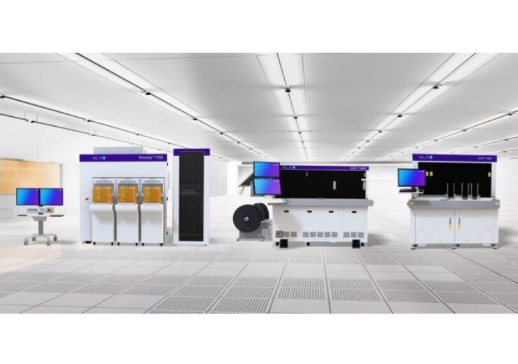
KLA’s new systems will help address a wide variety of IC packaging challenges. (Credit: KLA Corporation)
US-based equipment and services provider KLA has announced the launch of an enhanced portfolio of systems for advanced packaging applications.
The company has introduced the new Kronos 1190 wafer-level packaging inspection system, the ICOS F160XP die sorting and inspection system and the next-generation ICOS T3/T7 Series of packaged integrated circuit (IC) component inspection and metrology systems.
KLA’s new tools offer increased sensitivity, improved throughput and enhanced algorithms
Offering increased sensitivity, improved throughput and enhanced algorithms, the new tools will help advance semiconductor device fabrication at the packaging stage by solving the complexities of shrinking features sizes, 3D structures and heterogeneous integration.
The Kronos 1190 wafer inspection system uses high-resolution optics to offer inline process control for advanced wafer-level packaging process steps as features shrink and patterns become denser.
Its DefectWise system incorporates artificial intelligence (AI) as a system-level solution to enhance sensitivity, productivity and classification accuracy.
KLA’s ICOS F160XP system is used to conduct an inspection and die sorting after wafer-level packages are tested and diced.
The system features new IR2.0 inspection module that combines optical and true IR side inspection to increase the throughput for 100% IR inspection.
It offers an efficient inspection flow with high sensitivity that helps to minimise cracks and other defect types, as well as enables to precisely detect bad parts for maximum die sorting accuracy.
The next generation of the ICOS T3/T7 Series is available in several new configurations with fully automated optical IC component inspectors, which will help address varying inspection requirements across the packaging assembly process.
The increased sensitivity of inspectors in the series will help detect small defect types, while the precise and repeatable 3D metrology will help efficiently detect issues that affect final package quality.
KLA’s ICOS T3/T7 Series applies AI systems with deep learning algorithms to facilitate smarter binning of defect types and offer precise feedback on package quality to sort good and bad parts with less operator review across a range of device types and sizes.
KLA electronics, packaging and components (EPC) group executive vice president Oreste Donzella said: “Process control across all stages of packaging manufacturing, from wafer- to component-level process steps, becomes more critical as innovations continue to advance packaging technology.
“Our newly launched products help device manufacturers, foundries and outsourced semiconductor and test (OSAT) providers meet expectations for quality and reliability in an increasingly diverse and complex packaging segment.”