
The eSL10 e-beam inspection system features several revolutionary technologies that power its ability to close critical defect detection gaps
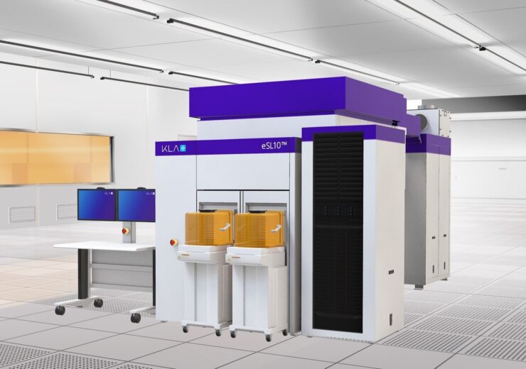
KLA’s electron-beam defect inspection system. (Credit: KLA Corporation)
KLA Corporation announced the revolutionary eSL10 e-beam patterned-wafer defect inspection system. The new system is designed to accelerate time-to-market for high-performance logic and memory chips, including those that rely on extreme ultraviolet (EUV) lithography, by detecting and reporting defects that cannot be routinely captured by optical or other e-beam defect inspection platforms. Built from the ground up, with multiple breakthrough technologies reflecting years of research and development, the eSL10 delivers high resolution, high speed inspection capability, unmatched by any other e-beam system on the market.
“With a single, high current-density electron beam, the eSL10 system has raised e-beam inspection performance to a new level,” said Amir Azordegan, general manager of the e-beam division at KLA. “Before now, e-beam inspection systems have offered either sensitivity or speed, severely limiting practical application. Our talented engineering team has taken an entirely new approach to e-beam architecture and algorithms, designing a system that can solve problems not addressed by existing tools. Today KLA is putting e-beam inspection on the list of equipment critical for leading-edge device manufacturing.”
The eSL10 e-beam inspection system features several revolutionary technologies that power its ability to close critical defect detection gaps. A unique electron optics design produces the industry’s widest operating range for defect capture across a variety of process layers and device types. Yellowstone scanning mode uses 10 billion pixels of information per scan to support high speed operation without compromising resolution, for efficient investigation of suspected hotspots or defect discovery within a broad area. Simul-6 sensor technology collects surface, topographic, material contrast and deep trench information in one scan, reducing the time required to identify different defect types within challenging device structures and materials. With its advanced Artificial Intelligence (AI) system, the eSL10 employs deep learning algorithms that adapt to IC manufacturers’ evolving inspection requirements, isolating the defects most critical to device performance.
Three-dimensional device architectures – such as 3D NAND and DRAM for memory, and finFET and gate all around (GAA) transistors for logic – are requiring fabs to rethink traditional defect control strategies. The combination of the eSL10 with KLA’s flagship 39xx (“Gen5”) and 29xx (“Gen4”) broadband optical wafer defect inspection systems creates a powerful defect discovery and monitoring solution for advanced IC technologies. Together these systems accelerate yield and reliability, finding critical defects faster and enabling quicker resolution of defect issues from R&D to production.
Extendibility is built in to the new eSL10 platform to allow for application expansion throughout the e-beam inspection and metrology space. Several eSL10 systems are in operation at leading logic, memory, and original equipment manufacturers worldwide, where they are helping to develop, ramp and monitor manufacturing of next-generation processes and devices. To maintain their high performance and productivity, eSL10 systems are backed by KLA’s global comprehensive service network. Additional information about the new e-beam defect inspection system can be found on the eSL10 product page.
Source: Company Press Release