
KLA has expanded its product portfolio with the introduction of new 392x and 295x optical defect inspection systems and the eDR7380 e-beam defect review system.
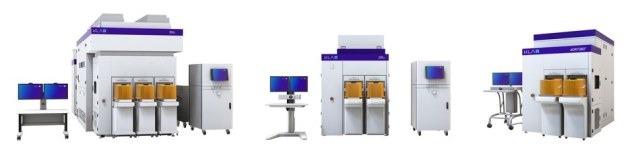
Image: KLA’s new 392x and 295x optical inspection systems and eDR7380 e-beam review system. Photo: courtesy of PRNewswire / KLA Corporation.
The new portfolio has been designed to accelerate time-to-market for major D NAND, DRAM and logic integrated circuits (ICs) across their product lifecycle.
The 392x and 295x optical patterned wafer defect inspection systems can leverage significant advances in broadband plasma illumination technology, sensor architecture and integration of chip design information.
KLA’s new systems will facilitate faster defect discovery, accelerated yield learning, and more comprehensive inline monitoring compared against major predecessors, said the company.
The 392x and 295x systems deploy different wavelength ranges to cover inspection applications for all layers, from shallow trench isolation through metallisation, including EUV lithography quality control.
KLA’s new eDR7380 e-beam wafer defect review system is said to offer quicker defect sourcing in development, faster excursion detection and more precise data during production.
According to the company, the system is equipped to support review of fragile EUV lithography process layers and its unique linkage to KLA inspectors reduces time to results and enables access to a range of KLA-specific applications, as well as enhances inspection sensitivity through smart sampling and efficient exchange of defect data.
The company is providing 392x, 295x and eDR7380 as new systems or as upgrades from previous-generation 39xx, 29xx or eDR7xxx systems.
KLA’s global comprehensive service network will support the 92x, 295x and eDR7380 systems to maintain the better performance and productivity of the chip manufacturers.
KLA global products group executive vice president Ahmad Khan said: “Device structures are smaller, narrower, taller and deeper, with more complex shapes and new materials. Discriminating defects from benign physical variations—signal from noise—has become an incredibly difficult problem.
“I’m excited to announce that our optical and e-beam engineering teams have developed a family of innovative, connected defect inspection and review systems, designed to enable our industry to continue to move forward.”
KLA provides advanced process control and process-enabling solutions for manufacturing wafers and reticles, integrated circuits, packaging, printed circuit boards and flat panel displays.