
Cadence Design Systems has announced that the complete Cadence advanced packaging design and analysis tool flow is certified by Samsung Foundry for fan-out panel-level-packaging (FO-PLP) and silicon-interposer 2.5D packaging.
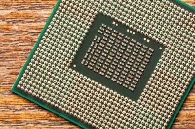
Image: Cadence’s proven on-/off-chip design flow is in use by multiple customers with challenging advanced packaging requirements. Photo: courtesy of Keattikorn / FreeDigitalPhotos.net.
This proven on-/off-chip design flow is in use now by multiple customers with challenging advanced packaging requirements.
Insuring sufficient, efficient and stable power delivery, as well as signal integrity, is a significant challenge for customers implementing advanced packages. With the advanced package reference flow, joint customers of Cadence and Samsung now have a documented step-by-step approach to validate these critical electrical requirements to enable first-pass success.
The complete Cadence advanced packaging flow is certified and correlated to the Samsung golden flow using Cadence on-/-off-chip power integrity and signal integrity tools, including Allegro Sigrity PowerSI technology, Sigrity Broadband SPICE, Sigrity PowerSI 3D-EM Extraction Option, Sigrity SystemSI technology, Sigrity System Explorer, Voltus IC Power Integrity Solution, Spectre Accelerated Parallel Simulator and Spectre CPU Accelerator Option.
This flow was verified with memory interfaces, high-speed interfaces and a core Power Delivery Network for CPU and GPU through both FO-PLP and Silicon-interposer 2.5D package-based test cases.
Cadence senior product engineering group director Steve Durrill said: “In close collaboration with Samsung, we have delivered a certified, integrated design and analysis flow for the Samsung Foundry advanced package design methodology.
“The Samsung certification of our solution that spans our Virtuoso, Allegro and Sigrity product lines enables our joint customers to take advantage of a reference flow that will help reduce cost and improve performance and reliability of their products using advanced packaging techniques.”
Samsung Electronics foundry marketing vice president Ryan Lee said: “We are pleased to see that the results from the Cadence analysis tools correlate with measurement results.
“This collaboration will help our customers with a trusted system design enablement solution for the advanced packages to implement state-of-the-art products.”
Source: Company Press Release